CEA LETI TECHNOLOGY RESEARCH INSTITUTE
Located in Grenoble, the capital of the French Alps, LETI is an institute dedicated to applied research in micro- and nano-technologies, information technologies, and healthcare technologies. LETI serves as a privileged interface between industry and academia. Through research programs utilizing world-leading technology platforms, it ensures the development and industrial transfer of innovative technologies across a wide range of sectors.
Research Area: Materials Characterization, Surface Techniques, Nano-electronics
PhD Topic Title: Quantification of Binary Compounds for Epitaxial Materials of Advanced Transistor Channels
Context: Within the European Chips Act, CEA-Leti is strongly committed to developing the next generation of fully-depleted silicon-on-insulator (FDSOI) transistor devices, which will enable faster and more energy-efficient processors. These technologies require novel process developments at all stages of device fabrication and the introduction of novel crystalline materials for the transistor channel with perfectly controlled elemental compositions. This presents significant challenges for characterization techniques in terms of precision and accuracy of the measurements performed and calls for new analytical strategies.
Work Required: The work will be performed at the Platform for Nanocharacterization of CEA-Leti, which gathers world-class analytical techniques and state-of-the-art instruments. The main objective of the thesis is to provide reliable support for the processing of front-end materials for advanced FDSOI technologies. To achieve this, methodologies for elemental quantification focused on the use of hard X-ray photoelectron spectroscopy (HAXPES) will be developed and validated through a collaborative framework at multiple levels, both internal and industrial. The targeted materials are primarily silicon and germanium compounds contributing to the optimization of the channels of advanced FDSOI transistors, such as Si, SiGe, and their derivatives (GeSn, SiGe). A combined analytical approach involving other nanoscale characterization techniques will be strengthened by identifying the most appropriate techniques to produce reference data (SIMS, RBS, etc.). In a third step, multi-scale aspects will be developed. In particular, they will aim to investigate to what extent the composition measured by HAXPES on a material developed upstream of transistor integration steps (for process deposition optimization) compares to that determined by other techniques (atom probe tomography, TEM) at the end of nanometric device integration.
Requested Background: Master’s degree in a relevant field
Duration: 36 months
Start Period: October 2024
Link to Offer: [Insert Link Here]
Host Laboratory: LETI/DPFT/SMCP/LASI
Address: 17, Avenue des Martyrs, 38054 Grenoble Cedex 9, France
Contacts:
- Nicolas Gauthier: nicolas.gauthier@cea.fr
Olivier Renault: olivier.renault@cea.fr
*Following is the full advertisement image provided.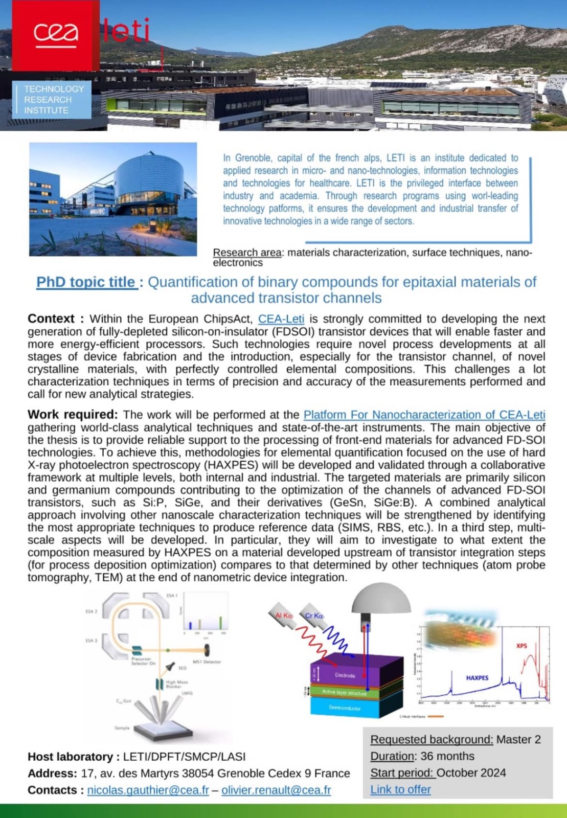
For more scholarship and assistantship update visit : gradassistantship
Feature photo credit: Wikipedia
If you have any inquiries or concerns about the content posted on our website, please do not hesitate to reach out to us via email (info.gradassistantship@gmail.com).